- 您现在的位置:买卖IC网 > Sheet目录405 > DMN21D2UFB-7B (Diodes Inc)MOSFET N CH 20V X1-DFN1006-3
�� �
�
�DMN21D2UFB�
�20V� N-CHANNEL� ENHANCEMENT� MODE� MOSFET�
�Product� Summary�
�Features� and� Benefits�
�?�
�Low� On-Resistance�
�V� (BR)DSS�
�20V�
�R� DS(ON)� max�
�0.99� ?� @� V� GS� =� 4.5V�
�1.2� ?� @� V� GS� =� 2.5V�
�2.4� ?� @� V� GS� =� 1.8V�
�3.0� ?� @� V� GS� =� 1.5V�
�I� D� max�
�T� A� =� 25°C�
�760mA�
�700mA�
�500mA�
�350mA�
�?�
�?�
�?�
�?�
�?�
�?�
�?�
�?�
�?�
�Very� low� Gate� Threshold� Voltage,� 1.0V� max�
�Low� Input� Capacitance�
�Fast� Switching� Speed�
�Ultra-Small� Surface� Mount� Package� 1mm� x� 0.6mm�
�Low� Package� Profile,� 0.5mm� Maximum� Package� height�
�ESD� Protected� Gate�
�Totally� Lead-Free� &� Fully� RoHS� Compliant� (Notes� 1� &� 2)�
�Halogen� and� Antimony� Free.� “Green”� Device� (Note� 3)�
�Qualified� to� AEC-Q101� standards� for� High� Reliability�
�Description� and� Applications�
�Mechanical� Data�
�This� MOSFET� has� been� designed� to� minimize� the� on-state� resistance�
�(R� DS(on)� )� and� yet� maintain� superior� switching� performance,� making� it�
�ideal� for� high� efficiency� power� management� applications.�
�?�
�?�
�Case:� X1-DFN1006-3�
�Case� Material:� Molded� Plastic,� "Green"� Molding� Compound.�
�UL� Flammability� Classification� Rating� 94V-0�
�?�
�?�
�?�
�General� Purpose� Interfacing� Switch�
�Power� Management� Functions�
�Analog� Switch�
�?�
�?�
�?�
�?�
�Moisture� Sensitivity:� Level� 1� per� J-STD-020�
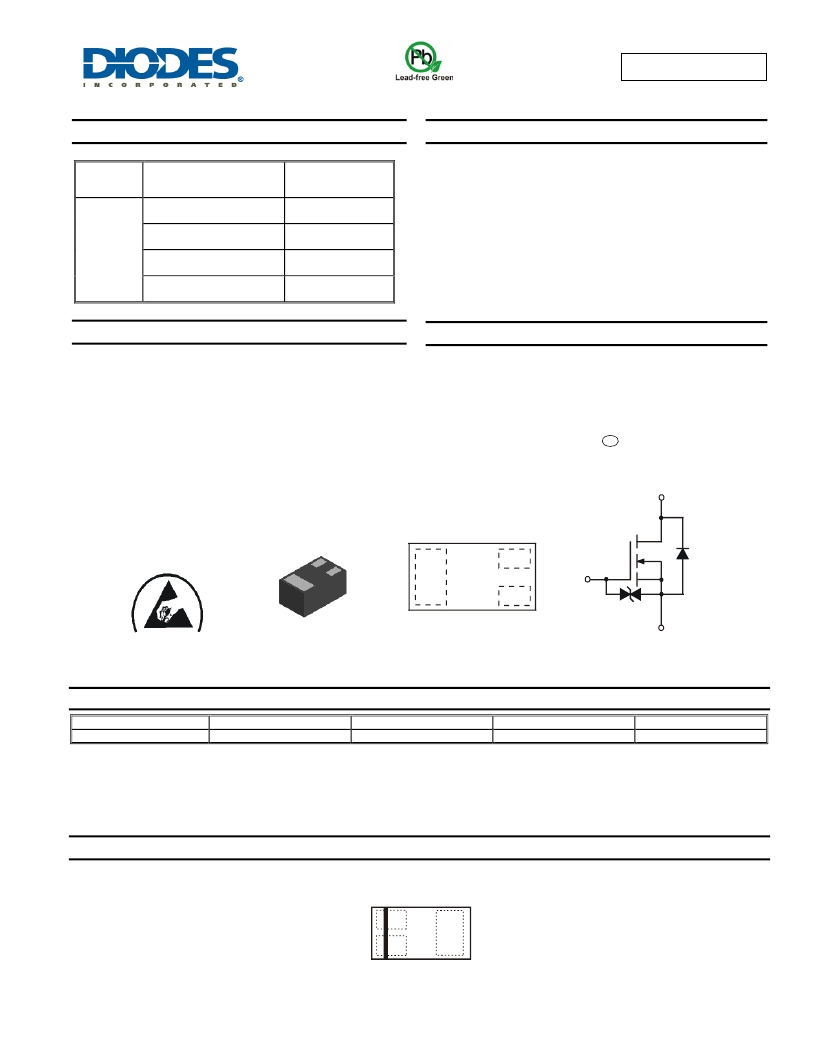
�Terminal� Connections� Indicator:� See� diagram�
�Terminals:� Finish� –� NiPdAu� over� Copper� leadframe.� Solderable�
�per� MIL-STD-202,� Method� 208� e4�
�Weight:� 0.001� grams� (approximate)�
�Drain�
�X1-DFN1006-3�
�Body�
�D�
�S�
�G�
�Gate�
�Gate�
�Diode�
�Source�
�ESD� PROTECTED�
�Bottom� View�
�Top� View�
�Package� Pin� Configuration�
�Protection�
�Diode�
�Equivalent� Circuit�
�Ordering� Information� (Note� 4)�
�Part� Number�
�DMN21D2UFB-7B�
�Marking�
�NN�
�Reel� size� (inches)�
�7�
�Tape� width� (mm)�
�8�
�Quantity� per� reel�
�10,000�
�Notes:�
�1.� No� purposely� added� lead.� Fully� EU� Directive� 2002/95/EC� (RoHS)� &� 2011/65/EU� (RoHS� 2)� compliant.�
�2.� See� http://www.diodes.com� for� more� information� about� Diodes� Incorporated’s� definitions� of� Halogen-� and� Antimony-free,� "Green"� and� Lead-free.� ?�
�3.� Halogen-� and� Antimony-free� "Green”� products� are� defined� as� those� which� contain� <900ppm� bromine,� <900ppm� chlorine� (<1500ppm� total� Br� +� Cl)� and�
�<1000ppm� antimony� compounds.�
�4.� For� packaging� details,� go� to� our� website� at� http://www.diodes.com.�
�Marking� Information�
�DMN21D2UFB-7B�
�NN�
�NN� =� Product� Type� Marking� Code�
�Top� View�
�Bar� Denotes� Gate� and� Source� Side�
�DMN21D2UFB�
�Document� number:� DS35564� Rev.� 5� -� 2�
�1� of� 6�
�www.diodes.com�
�May� 2012�
�?� Diodes� Incorporated�
�发布紧急采购,3分钟左右您将得到回复。
相关PDF资料
DMN2215UDM-7
MOSFET N-CH 20V 2A SOT-26
DMN2230U-7
MOSFET N-CH 20V 2A SOT23-3
DMN2300U-7
MOSFET N-CH 20V 1.24A SOT23
DMN2300UFB4-7B
MOSF N CH 20V 1.3A DFN1006H4-3
DMN2300UFD-7
MOSFET N-CH 20V 1.73A 3UDFN
DMN2400UFB-7
MOSF N CH 20V 750MA X1-DFN1006-3
DMN2400UFB4-7
MOSFET N-CH 20V 750MA DFN1006H4
DMN2400UV-7
MOSFET 2N-CH 20V 1.33A SOT563
相关代理商/技术参数
DMN2215UDM
制造商:DIODES 制造商全称:Diodes Incorporated 功能描述:DUAL N-CHANNEL ENHANCEMENT MODE FIELD EFFECT TRANSISTOR
DMN2215UDM-7
功能描述:MOSFET 650mW 20V RoHS:否 制造商:STMicroelectronics 晶体管极性:N-Channel 汲极/源极击穿电压:650 V 闸/源击穿电压:25 V 漏极连续电流:130 A 电阻汲极/源极 RDS(导通):0.014 Ohms 配置:Single 最大工作温度: 安装风格:Through Hole 封装 / 箱体:Max247 封装:Tube
DMN2230U
制造商:DIODES 制造商全称:Diodes Incorporated 功能描述:N-CHANNEL ENHANCEMENT MODE FIELD EFFECT TRANSISTOR
DMN2230U-7
功能描述:MOSFET 600mW 20Vdss RoHS:否 制造商:STMicroelectronics 晶体管极性:N-Channel 汲极/源极击穿电压:650 V 闸/源击穿电压:25 V 漏极连续电流:130 A 电阻汲极/源极 RDS(导通):0.014 Ohms 配置:Single 最大工作温度: 安装风格:Through Hole 封装 / 箱体:Max247 封装:Tube
DMN2250UFB-7B
制造商:Diodes Incorporated 功能描述:MOSFET BVDSS: 8V-24V X1-DFN1006-3 T&R 10K - Tape and Reel 制造商:Diodes Incorporated 功能描述:MOSF N CH 20V 1.35A X1DFN10063 制造商:Diodes Incorporated 功能描述:MOSFET N-channel 20V 1.35A DFN1006-3
DMN2300U
制造商:TYSEMI 制造商全称:TY Semiconductor Co., Ltd 功能描述:20V N-CHANNEL ENHANCEMENT MODE MOSFET IN SOT23 ESD Protected Gate 2kV
DMN2300U-7
功能描述:MOSFET MOSFET BVDSS: 8V-24V SOT23,3K RoHS:否 制造商:STMicroelectronics 晶体管极性:N-Channel 汲极/源极击穿电压:650 V 闸/源击穿电压:25 V 漏极连续电流:130 A 电阻汲极/源极 RDS(导通):0.014 Ohms 配置:Single 最大工作温度: 安装风格:Through Hole 封装 / 箱体:Max247 封装:Tube
DMN2300UFB
制造商:DIODES 制造商全称:Diodes Incorporated 功能描述:20V N-CHANNEL ENHANCEMENT MODE MOSFET